Simulate
DC drop and thermal
Solve every copper layer for voltage drop and current density, then the board’s temperature with each part’s power, in seconds.
DC drop and thermal sims answer the two questions every power path raises: does the load see the voltage it needs, and how hot does the board get. Both run in seconds, so run them freely, after every layout change that touches a power path.
DC drop
name = "lna-dc"
kind = "dc"
layout = "lna"
cell = 0.05

[[supplies]]
pad = "D2.1"
voltage = "4.7V"

[[supplies]]
pad = "J3.2"
voltage = "0V"

[[loads]]
pad = "U1.3"
current = "90mA"
return = "U1.2"

[[links]]
ref = "L1"
resistance = "0.6ohm"
The solver treats the copper of every layer as a resistive sheet, with vias as plated barrels between the layers they span, holds the supply pads at their voltage and draws each load's current out at its pad and back in at its return. It solves the whole board in double precision by sparse Cholesky.
Parts carry DC through [[links]]. Resistors take their value from the schematic; inductors and ferrite beads default to 0.1 ohm, so give a choke its datasheet DCR, as above. Anything else is open unless linked. A link joins pads 1 and 2 unless a and b name others, so a load switch is { ref = "U5", resistance = "80mohm", a = "1", b = "6" }.
agentee sim lna-dc
agentee show sim:lna-dcsupply D2.1 4.7 V sources 90.00 mA
load U1.3 4.645 V 90 mA, pad 4.6453 V, return 0.0000 V
peak current density 13.892 A/mm2 F.Cu at [16.15, 12.10]
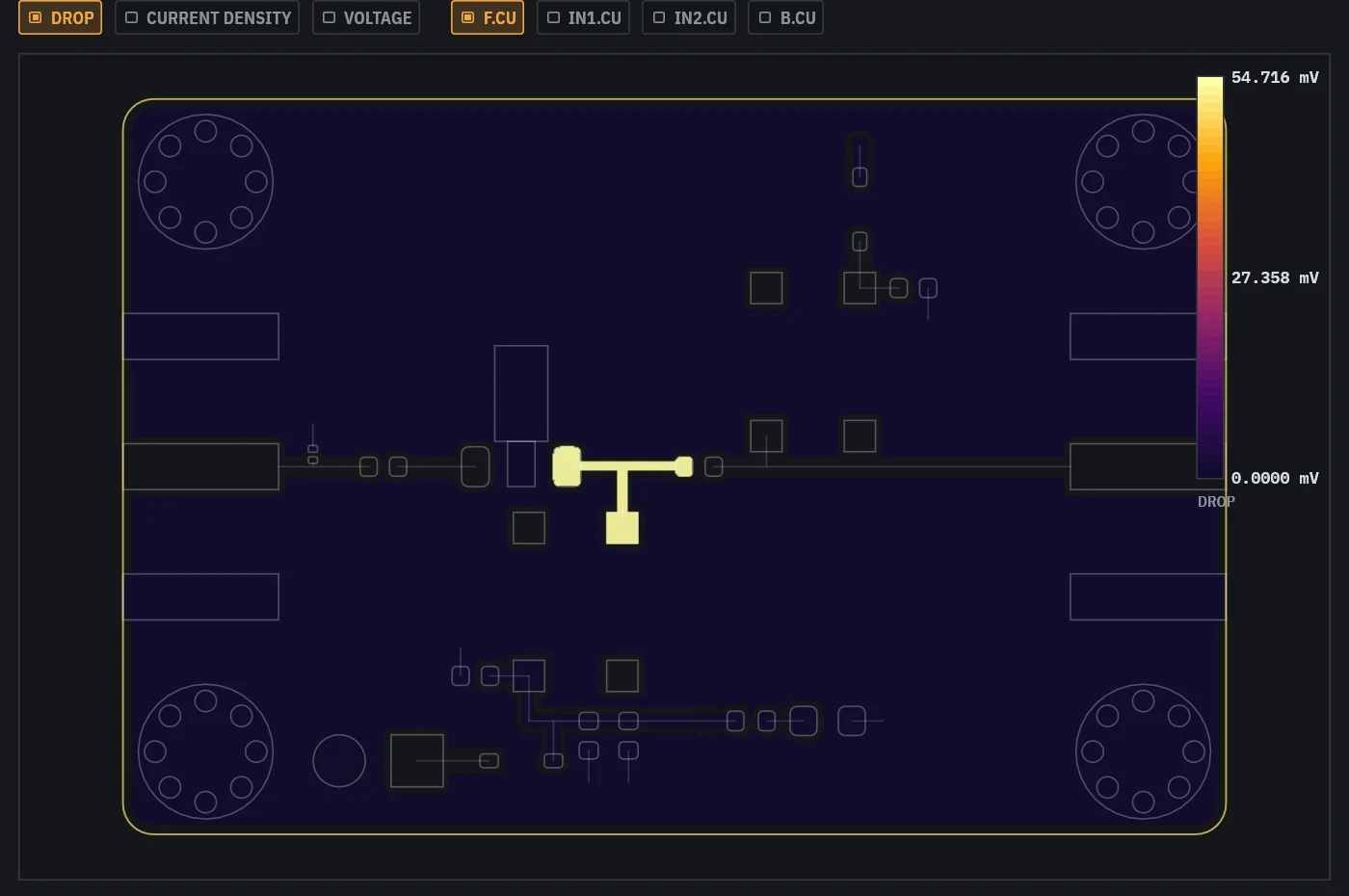
via [12.55, 11.00] 5.575 mA busiest viasThat run took two seconds. The maps show the drop from each copper island's supply in mV, the current density in A/mm2 and the voltage. Look at the density map for necks: a pour squeezed between two pads, or a single via carrying a rail.
Thermal
name = "lna-thermal"
kind = "thermal"
layout = "lna"
cell = 0.2
ambient = 25.0

[[sources]]
ref = "U1"
power = "0.45W"
theta_jc = 65.0
pads = ["2"]

[[sources]]
ref = "D2"
power = "30mW"
Steady state conduction through FR4 (0.8 W/mK in plane, 0.3 through), the copper sheets and the via barrels, with convection from both faces, solved on the GPU by preconditioned conjugate gradient. A source puts its power into the board through its pads, or only through the pads you name, like a regulator's thermal tab. theta_jc adds a junction estimate on top of the pad temperature.
board peak     60.2 C   F.Cu at [13.00, 11.60]
U1 pads        60.2 C   0.45 W
U1 junction    89.4 C   pads + 0.45 W x 65 C/W
D2 pads        57.4 C   0.03 W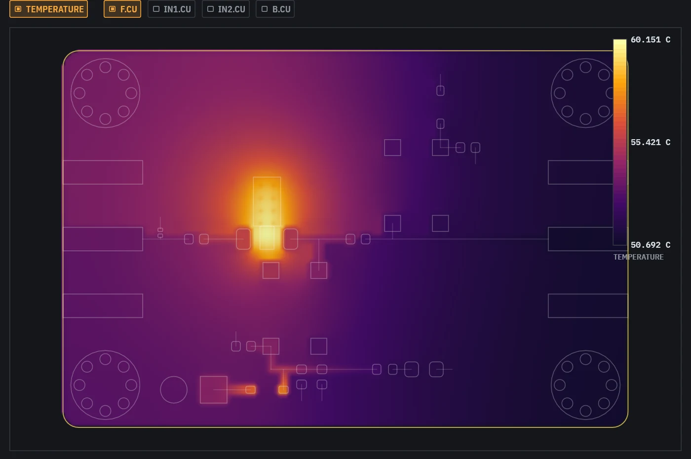
Model the enclosure
h_top and h_bottom are the convection coefficients of each face, in W/m2K: 10 is still air, 25 and up with a fan. A face pressed onto a heatsink or baseplate through a gap pad is a much larger number. The LNA's second thermal sim puts the whole bottom on a 1 mm, 3 W/mK gap pad to a 70 C baseplate:
name = "lna-thermal-chassis"
kind = "thermal"
layout = "lna"
ambient = 70.0
h_bottom = 3000.0board peak 76.8 C
U1 pads 76.8 C 0.45 W
U1 junction 106.0 CThe SPF5189Z is rated to an 85 C lead temperature, so this is the run that says whether the design works in its box. Write that reasoning into the sim's description, as the example does: the next person, or the next agent session, reads it there.
When to run them
- After placing a regulator, an amplifier or anything over a quarter of a watt. The placer reads the thermal sims of a layout and keeps their sources at 0.25 W and up apart.
- After routing a rail, to catch a neck before it becomes a hot spot.
- Before ordering, with the real enclosure.
Results go stale when the spec or the copper changes, and check says so.